|
Transistor
Substitution
|
|
De-soldering and replacing a transistor takes very little time.
More time is spent figuring out which one to replace and, sometimes,
what to replace it with!
The original transistor might need special ordering, or be discontinued and unavailable. Knowing how to
substitute an alternate transistor type can speed up your repair, or
make an otherwise impossible repair possible.
|
Transistor Types
|
Transistors are given registered type numbers by the Joint Electron Device
Engineering Council (JEDEC). The type number is often printed on the
transistor, although product manufacturers sometimes have their own part numbers printed
instead. In that case, the product's Service Manual or Parts List might provide
you with the transistor type.
If you don't have that particular type, a transistor cross-reference
book can sometimes help you to find a compatible part. But you might already have a suitable substitute in your parts drawers.
We arrange our transistor stock, not by their type number, but by their
specifications This makes it easy to go right to the drawers
holding good candidates for substitution.
You can find transistor specs in data sheets available online.
Use your browser to search for the transistor's JEDEC type, or use a search engine like
AllDataSheet.com.
The first spec to consider is the Transistor Outline. This is the only
spec you can actually see.
|
Transistor Outlines
|
A Transistor Outline number, or TO, refers to a transistor's
physical size, shape, and
mounting style. Some TO numbers are shown here:
|
The transistor outline doesn't usually tell you which of the three transistor leads
connects to its Base terminal (B), its Emitter terminal (E), or its Collector terminal (C).
However, the transistor's data sheet will show you that.
If the lead arrangement of a small replacement transistor differs from
that of the original, you can sometimes bend the transistor leads across one another to route them into the
correct holes in the circuit board. Just use a bit of spaghetti tubing
on the leads to keep them from touching each other.
|
Bipolar Transistors (BJTs)
|
The "bipolar transistor", technically a "bipolar junction transistor" or BJT,
is a common variety of transistor.
"Bipolar" transistors use both electrons and holes (electron vacancies) as charge carriers.
The following electrical specs are important when choosing a substitute BJT.
|
Polarity
|
"Junction" transistors exploit the behavior of junctions between "N-type" and
"P-type" semiconductors. N-type semis contain excess electrons
while P-type semis contain excess
holes.
"NPN" transistors sandwich a P region between two N
regions, creating two junctions. Similarly, "PNP" transistors
sandwich an N region between
two P regions.
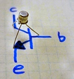
The central region is called the base (symbol B). A small current
between the emitter (symbol E) and the base controls a larger current
between the emitter and the collector (symbol C).
A substitute transistor must have the same polarity (NPN or PNP) as the
original. If it has the wrong polarity, it won't work properly
in it's circuit.
|
Maximum Voltages
|
If more than a maximum voltage rating is applied to a transistor, it
can be permanently damaged. At the maximum voltage, also called a breakdown voltage
(BV), electrons begin to avalanche in the transistor.
During an avalanche, electrons in the P-N transition regions are
accelerated to energies so high that they hit bound electrons with
enough force to free them, creating additional
charge carriers and greatly multiplying the
transistor current.
There are three breakdown voltages:
-
VCB - the maximum voltage across the Collector-Base terminals
-
VCE - the maximum voltage across the Collector-Emitter terminals
-
VEB - the maximum voltage across the Emitter-Base terminals
In each of these ratings, the 3rd terminal is assumed to be
electrically Open (unconnected). VCE,
for example, may be written as VCEO, BVCEO, or
most correctly as V(BR)CEO.
The VEB rating isn't usually a factor
in choosing a substitute transistor.
VCB is always equal to or greater than VCE
and you can
use either of these maximum voltages to compare transistors. Choose
a substitute transistor with a breakdown voltage rating at least as high as the original.
|
Maximum Current
|
Maximum current is the maximum continuous collector current (IC)
that a transistor can withstand without permanent damage.
Small, TO-92 or TO-98 transistors, depending on their fabrication, can handle between about
100 and 1000 mA. A TO-5 package
might be rated as high as 5 amps; a TO-220, as high as 25 A; and a TO-3, up to 500 A.
Be sure to choose a substitute transistor with a maximum current rating at least as high
as the original.
|
Maximum Power
|
Maximum Power, called PD, is the overall power a transistor can dissipate, through
heat, without burning up.
Heat sinks and fans increase the ability of a transistor to dissipate
heat. A TO-5 transistor with a PD of
3 watts might be able to dissipate 8-10 watts with a heat sink.
Choose a substitute transistor with a maximum power rating at least as high as the original.
|
Current Gain
|
Current gain is only occasionally significant when choosing a substitute transistor.
Actual circuit gain depends on other components. But if the
original transistor has a high gain, try to match it.
Current gain falls off at higher frequencies, so a high-gain transistor can
deliver a wider frequency response than a low-gain transistor.
One measure of gain, called hFE, is often used for
comparing transistors. The capital FE subscript refers to
the
Forward DC current transfer ratio in a common
Emitter circuit. In other words, IC / IB.
Data sheets often specify a minimum or typical value of hFE,
or else a range of values that applies at a certain collector current (IC).
"Darlington" transistors are made up of two transistors in series
and have gains in the thousands, instead of the tens or hundreds. They also have double
the input voltage drop since there are two semiconductor junctions in series.
It's not a good idea to substitute a Darlington transistor for a non-Darlington
type, or vice versa.
|
Field-Effect Transistors (FETs)
|
Field-effect transistors (FETs) use an
electric field to control charge flow through a conduction channel.
As with BJTs, the gate (symbol G) is the terminal that controls the
transistor current.
However, in a FET, the controlled current flows between the
transistor's source (symbol S) and its drain (symbol D).
FETs are unipolar,
not bipolar, using either electrons or holes as charge carriers, but not both.
FETs are built into the same transistor outlines as BJTs but their
electrical specs differ:
|
FET Types
|
Field-effect transistors come in three basic types:
-
Type A - the
Junction-gate FET (JFET)
-
Type B - the Insulated-gate FET (IGFET) in
"depletion mode"
-
Type C - the Insulated-gate FET (IGFET) in
"enhancement mode"
IGFETs are commonly called MOSFETs (Metal-Oxide-Semiconductor FETs) because, originally, all
insulated-gate FETs
had metal gates coated with oxide insulation.
FET acronyms now abound but they
only describe how a FET is constructed or improved; they don't define
a new basic type.
Each type of FET can be fabricated with either an N-type or a P-type
conduction channel. So, overall, there are six types of field-effect transistors.
Following are their circuit symbols:
|
Be sure to substitute a FET of the same type as the original.
|
Maximum Voltages
|
One of the following breakdown voltages is usually included in the specifications for a FET:
-
BVGSS - the breakdown voltage between the Gate and the
Source terminals when the drain is short-circuited to
the source. (This rating is used primarily with JFETs.)
-
BVDSS - the breakdown voltage between the Drain and
the Source terminals when the gate is short-circuited to the source.
(This rating is used primarily with Power MOSFETs.)
A breakdown voltage can also be written as V(BR)GSS or
simply VGSS.
You can use either of the above voltages when comparing FETs. Just
make sure to compare apples with apples. Pick a substitute FET with a rating at least as high as the original.
|
Current
|
IDSS is the Drain to Source leakage current, often provided for small-signal FETs.
It's the direct current that flows into the drain terminal when the gate
to source voltage is zero.
In a depletion type device, IDSS is an on-state current. In an
enhancement type device, it's an off-state current.
Minimum and maximum values are usually given. Select a substitute with the same general range of values.
ID(cont), the Continuous Drain Current, is usually
provided for power MOSFETs. It's a maximum current rating so choose a substitute
with a rating at least as high as the original.
|
Maximum Power
|
PD is the overall power the FET can dissipate through heat.
This is the same spec used for bipolar transistors. Choose a substitute
with a rating at least as high as the original.
|
"On" Resistance
|
rDS(on) is the DC
resistance between the Drain and Source terminals when a specified
gate to source voltage is applied to bias the FET to the on-state.
For a depletion-type FET, the gate to source bias voltage might be 0 V (i.e., a
gate to source short).
rDS(on) could be important when replacing a power MOSFET.
|
Summary
|
Finding a substitute replacement transistor isn't difficult if you know
the specs of the original transistor and organize your stock by specs instead of type numbers.
You'll find that fewer devices need to be stocked, and turnaround time can be reduced.
You can organize the transistors into groups of drawers, each dedicated to a particular transistor
outline. Subdivide the TO groups by electrical ratings like VCEO,
IC, and PD, in whatever order you choose.
Then, when you need to pick a substitute for an original transistor, you can quickly
home in on all
your potential candidates.
|
|
|